Introduction to the Power of 266nm Lasers
In the world of photonics and laser technology, the 266nm laser has emerged as a cornerstone for various applications. It’s not just about the mere existence of this wavelength but understanding how its unique characteristics are revolutionizing industries.
A Dive into Short Wavelengths
When delving into the fascinating world of lasers and light technologies, it becomes evident that not all wavelengths are created equal. Among the multitude, the 266nm wavelength stands distinct, offering unique advantages and characteristics that set it apart. This wavelength emanates from the ultraviolet (UV) light spectrum. As a point of reference, imagine the vast electromagnetic spectrum; here, nestled between the realms of the visible light that our eyes perceive and the mysterious X-rays, lies the ultraviolet spectrum. Within this UV spectrum, the 266nm wavelength is classified under deep ultraviolet, a segment known to exhibit high-energy photons.
These photons are not just regular packets of energy. Their high-energy nature allows them to interact with materials in ways that longer wavelengths cannot. They can be absorbed more readily, excite electrons with ease, and even break chemical bonds. Such capabilities are the reasons behind the success of UV lasers in applications ranging from sterilization to lithography.
But what truly distinguishes the 266nm laser from its counterparts is its incredible resolution. To understand this, one needs to consider a foundational principle of optics. This principle states that the ability of any optical system, be it a magnifying glass, a telescope, or a laser apparatus, to distinguish between close but separate entities, known as its resolution, is inversely related to the wavelength it employs. In simpler terms, the shorter the wavelength, the finer the detail it can discern. Given that the 266nm laser has a shorter wavelength, it boasts an outstanding resolution, making it the tool of choice for tasks requiring impeccable detail and unmatched precision.
This high-resolution capability of 266nm lasers is not just theoretical; it manifests in real-world applications. From the intricate patterns in semiconductor chips to the delicate artworks in glass etching, this laser’s superior resolution ensures that every minute detail is captured and reproduced flawlessly. In industries where a micron-level mistake can lead to substantial financial losses or in scientific experiments where precision is paramount, the 266nm laser proves to be indispensable.
In conclusion, the world of short wavelengths, particularly the 266nm range, offers profound insights and applications in modern technology. By understanding and harnessing its unique properties, industries can push the boundaries of what’s achievable, ushering in innovations that were previously thought impossible.

Harnessing 266nm Lasers in Precision Microfabrication
Precision microfabrication has revolutionized many industries, propelling them to new heights with the intricate and sophisticated components they can now produce. At the heart of this revolution lies the 266nm laser, an exceptional tool known for its unmatched accuracy and precision.
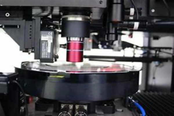
In the realm of ultra-precise manufacturing, the capabilities of the 266nm laser truly shine. Its short wavelength, as mentioned earlier, equates to high resolution. This, when translated to the manufacturing world, means the ability to create complex and detailed components that were previously inconceivable. Consider micro-electromechanical systems (MEMS), for instance. These tiny devices, often smaller than a grain of sand, integrate both mechanical and electrical components. Crafting such devices requires an incredibly high degree of precision, and the 266nm laser, with its fine detail capabilities, is just the tool for the job. Similarly, when creating semiconductor wafers, which are the foundation of our modern electronics, the precise etching and doping processes are made possible with the 266nm laser. Every transistor, every diode, every tiny component etched onto these wafers benefits from the laser’s unmatched precision.
But precision isn’t the only card the 266nm laser has up its sleeve. A significant challenge in microfabrication is managing the heat generated during manufacturing processes. Excessive heat can warp, melt, or otherwise damage the tiny components being crafted. Enter the 266nm laser and its attribute of reduced heat damage. Due to the high absorption rates of UV wavelengths in many materials, when the 266nm laser is used, it facilitates a much faster processing time. The laser’s energy is quickly absorbed, achieving the desired effect without lingering long enough to generate excessive heat. This rapid in-and-out approach minimizes heat generation and, by extension, reduces potential thermal damage. As a result, even the most delicate and intricate of microstructures remain intact and undamaged, ensuring that the final product functions as intended without any compromises.
Incorporating the 266nm laser in precision microfabrication has, thus, set a new benchmark in manufacturing. By marrying precision with safety, it ensures that the products of tomorrow are not only sophisticated but also reliable.
Materials Processing with 266nm Lasers
In the dynamic world of materials processing, lasers have long been an invaluable tool. But even among lasers, the 266nm variety stands out, primarily due to its unique properties that make it ideal for a range of applications, from the highly technical realm of semiconductor fabrication to the more routine processes of surface modification.
Diving deep into the intricacies of semiconductor manufacturing, one cannot ignore the pivotal role of photolithography. This process is akin to creating a blueprint for a city on a micro-scale. It involves projecting intricate patterns onto a substrate, which then guides subsequent etching and doping processes. Now, the quality of this “blueprint” dictates the efficiency, reliability, and size of the final semiconductor. And this is where the 266nm laser comes into play. Its short wavelength means it can produce finer details, allowing for the design of more compact and efficient circuits on semiconductor wafers. Think of it as the difference between drawing with a fine-tipped pen versus a broad marker. The former, represented by the 266nm laser, allows for much more detail and precision. Thus, in the realm of photolithography, the 266nm laser isn’t just a tool; it’s an enabler, pushing the boundaries of what’s possible in semiconductor manufacturing.
Shifting our attention from the microscopic scale of semiconductors to broader applications, we find the 266nm laser again proving its mettle in surface modification. Materials, be they metals, glasses, or polymers, often require surface treatments for various reasons, from aesthetic considerations to functional enhancements. Etching intricate designs, cleaning surfaces to remove contaminants, or even subtly modifying a material’s properties are tasks that demand precision. The 266nm laser, with its ability to interact primarily at the surface level without delving deep, is tailor-made for these applications. Its interactions are mostly superficial, making processes like etching incredibly precise. For instance, when cleaning a surface, the laser selectively targets and removes contaminants without harming the underlying material. This delicate and targeted interaction ensures that materials not only look better post-treatment but also exhibit enhanced properties, be it improved conductivity, reflectivity, or even enhanced resistance to wear and tear.
In essence, the 266nm laser is redefining materials processing, bridging the gap between what’s desired and what’s achievable, ensuring that industries are equipped with the best tools to drive innovation and enhance product quality.

UV Spectroscopy: A Game Changer with 266nm Lasers
Ultraviolet (UV) spectroscopy, a revered technique for decades, is integral to various scientific endeavors. It’s a method that unravels the mysteries of molecules by studying how they interact with light. And while UV spectroscopy is inherently potent, introducing the 266nm laser into the mix propels its capabilities to unparalleled heights.
A cornerstone of UV spectroscopy’s efficacy is its sensitivity, and this is where the 266nm laser makes its mark in enhanced sensitivity in molecular analysis. At its essence, spectroscopy hinges on the principle of exciting molecules using light, then analyzing the light they emit or absorb. The 266nm laser’s unique wavelength, being part of the deep ultraviolet spectrum, can excite a specific set of molecules that might remain unresponsive to other wavelengths. When these molecules are excited, they yield spectral data that is incredibly detailed. Such detail facilitates a richer and more comprehensive understanding of the molecule’s structure, behavior, and interactions. Imagine trying to understand a piece of music by hearing just a few notes versus experiencing the entire symphony. With the 266nm laser, scientists are privy to the full symphony of molecular data, enabling accurate, sensitive, and nuanced molecular analysis.
Beyond sensitivity, the realm of detection is another domain where the 266nm laser revolutionizes UV spectroscopy, leading to improved detection limits. Detecting substances, especially in trace amounts, can often be analogous to searching for a needle in a haystack. But with the 266nm laser, this search becomes markedly easier. The laser’s exceptional ability to excite specific molecules means even minuscule amounts, which might go unnoticed under other circumstances, become detectable. This heightened detection capability is invaluable in myriad fields. Consider forensic science, where identifying a trace of a substance could be the key evidence in solving a crime. Or environmental monitoring, where spotting infinitesimal amounts of pollutants can inform crucial ecological decisions. Not to forget pharmaceutical quality control, where ensuring the purity of drugs is paramount for patient safety. In all these fields, the razor-sharp detection offered by the 266nm laser is not just beneficial; it’s transformative.
In UV spectroscopy, while light and molecules have always danced together to reveal scientific truths, the 266nm laser has fine-tuned this dance, ensuring that every step, every move, and every twirl is executed with unparalleled precision and clarity.

Interaction with Matter: A Short Wavelength Marvel
When it comes to understanding how lasers interact with various materials, the wavelength is a primary determinant. Each wavelength offers unique capabilities, and the 266nm is no exception. Its properties make it a marvel when understanding its role in material processing and modification.
Diving into the realm of absorption, the 266nm laser showcases exemplary behavior with high absorption rates in many materials. In essence, absorption rates dictate how readily a material takes in the laser’s energy. A high absorption rate, as seen with the 266nm wavelength, means that the material rapidly and efficiently harnesses the laser’s power. Such quick and comprehensive absorption is pivotal in several industrial and scientific processes. For instance, when engraving intricate designs onto a substrate, the high absorption ensures that the laser’s energy is utilized optimally, leading to crisp and precise engravings. Similarly, in cutting or marking operations, this efficient energy uptake translates to clean cuts and vivid marks, with reduced chances of material wastage or inadvertent damage.
Furthermore, the efficiency of the 266nm laser isn’t just about how it delivers energy but also where. This laser is adept at controlled depth of interaction. Because of its high absorption rates, the energy doesn’t penetrate too deeply, ensuring that most of the interaction is at the surface level. This characteristic is particularly advantageous when the goal is to modify or treat just the surface without tampering with the underlying layers. Consider delicate operations, like modifying the surface texture of biomedical implants or adding protective coatings to precision instruments. In such applications, it’s crucial to make precise alterations without compromising the material’s bulk properties. The 266nm laser, with its surface-focused interactions, is the ideal tool for such tasks, ensuring that modifications are both effective and restricted to where they are needed most.
In summary, the 266nm laser’s interaction with matter is a testament to the wonders of short wavelengths. Its efficiency and precision make it an invaluable tool in the ever-evolving landscape of material science and engineering.
Conclusion
The 266nm laser, with its short wavelength, is proving to be a versatile tool that offers unparalleled advantages across a spectrum of industries. From precision microfabrication to the nuanced world of UV spectroscopy, its potential is vast. As technology continues to advance, the role of 266nm lasers is sure to become even more prominent, ushering in new innovations and achievements.
FAQs
- 1. How does the 266nm laser wavelength differ from other UV lasers?
The 266nm laser wavelength is considered deep ultraviolet, which means it offers higher energy photons, leading to enhanced resolution and detailed interactions with materials. - 2. Why is reduced heat damage essential in precision microfabrication?
Reduced heat damage ensures that delicate microstructures maintain their integrity, preventing any deformities or structural weaknesses. - 3. How does the 266nm laser improve the photolithography process?
The 266nm laser’s enhanced resolution allows for the fabrication of smaller and more efficient semiconductors, crucial in advancing electronic technology. - 4. What makes the 266nm laser ideal for surface treatments like etching?
The laser’s high absorption rates and controlled depth of interaction make it perfect for precise surface modifications without affecting deeper layers. - 5. Why is the detection limit important in UV spectroscopy?
A better detection limit means even trace amounts of substances can be identified, which is pivotal in many scientific and industrial applications.