Introduction
In the realm of materials science, the relationship between a crystal’s structure and its optical properties is of paramount importance. This article delves deep into the intricate connection between the two, shedding light on how the atomic arrangement within a crystal influences its ability to interact with light.
Understanding Crystal Structure
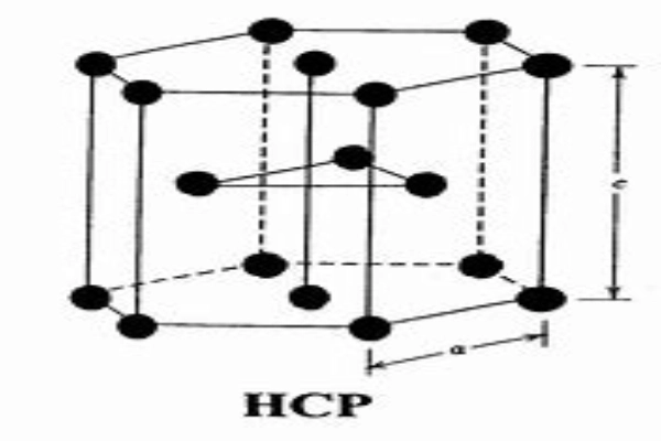
Understanding the structure of crystals is akin to deciphering the blueprint of nature’s intricate designs. At the heart of this structure lies the crystal lattice, a mesmerizing and repetitive pattern of atoms or molecules.
This isn’t just a mere arrangement; it’s the very foundation that imparts a crystal its distinctive shape and attributes. Imagine a vast hall filled with dancers, each repeating a specific set of steps in perfect harmony. This dance floor, in essence, represents the crystal lattice, where each dancer symbolizes an atom or molecule, moving and aligning in a predefined manner.
Now, if we were to zoom in further, focusing on a small group of dancers performing a particular sequence, we’d find a pattern that repeats itself throughout the hall. This specific sequence is what scientists refer to as the ‘unit cell’. It’s the fundamental building block of the crystal, much like how a brick is to a massive wall. Every crystal lattice is made up of countless unit cells, all meticulously arranged in three-dimensional space.
But what makes these unit cells truly fascinating is their inherent symmetry. Just as how symmetry in architecture can lead to aesthetically pleasing structures, in the realm of crystals, it dictates their overall properties. The way these unit cells are oriented and how they mirror each other plays a crucial role in determining not just the physical appearance of the crystal, but also its chemical and optical properties.
For instance, the symmetry in some crystals might lead to them being optically active, meaning they can rotate the plane of polarized light passing through them. Others, due to their unique unit cell arrangements, might exhibit piezoelectric properties, where they generate an electric charge in response to mechanical stress.
Furthermore, the arrangement of these unit cells can also influence the crystal’s mechanical strength, electrical conductivity, and even its thermal properties. It’s like a domino effect; a slight alteration at the unit cell level can lead to significant changes in the crystal’s overall behavior.
In essence, the world of crystals is a testament to nature’s meticulous craftsmanship. The lattice and unit cells are nature’s way of ensuring order, symmetry, and functionality. By understanding these fundamental aspects, we not only gain insight into the beauty of the natural world but also harness the potential of crystals in various scientific and technological applications.

Optical Properties of Crystals
The realm of optics and the world of crystals intertwine in ways that are both profound and intricate. When light, a form of electromagnetic radiation, encounters a crystal, a myriad of interactions can occur, leading to phenomena that are not only scientifically intriguing but also visually captivating.
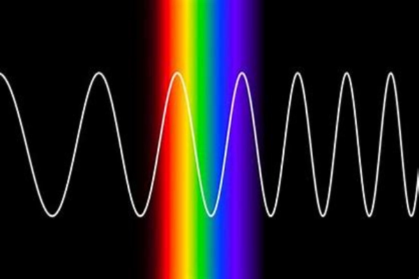
Take, for instance, the refractive index. At its core, this property encapsulates the crystal’s ability to bend or refract light. Imagine a beam of light, traveling at breakneck speed, suddenly entering a dense forest (the crystal). As it navigates through the trees (atoms and molecules), its pace slows down, and its path may alter.
This change in speed and direction is quantified by the refractive index. Factors such as the density of the forest and the arrangement of trees play a pivotal role in determining how much the light slows down. In the context of crystals, the denser the atomic or molecular arrangement, the higher the refractive index, leading to a greater bending of light.
However, not all light traverses through a crystal smoothly. Sometimes, it faces obstacles, much like a traveler encountering boulders or pits on a path. These obstacles in a crystal are the imperfections or irregularities in its lattice. When light meets these imperfections, it doesn’t just push through; it scatters, darting in multiple directions.
This scattering phenomenon can lead to effects like the iridescence observed in opals or the shimmer in certain minerals. The beauty one observes is essentially light playing games, bouncing off, and scattering due to the crystal’s imperfections.
Yet, another captivating optical property of crystals is their ability to absorb light. Not all wavelengths of light get the green signal to pass through a crystal. Some are selectively absorbed, and this selective absorption is what often imparts color to the crystal.
Think of it as a crystal having a preference for certain tunes in the vast symphony of light. The notes it doesn’t favor are absorbed, and what remains gives the crystal its characteristic hue. This absorption is not random; it’s governed by the crystal’s electronic structure. The way electrons are arranged and how they interact with light determines which wavelengths get absorbed and which pass through.
In essence, the dance of light within the confines of a crystal is a spectacle of nature. Whether it’s bending, scattering, or getting absorbed, these interactions reveal the intricate and delicate relationship between light and matter, painting a vivid picture of the universe’s microscopic wonders.
How Crystal Structure Influences Optical Properties
The intricate relationship between a crystal’s structure and its optical properties is a testament to the marvels of nature’s design. At the atomic level, the arrangement of atoms in a crystal lattice acts as a gatekeeper for light. Depending on this arrangement, light can be allowed to pass through, be blocked entirely, or even be redirected along a different path.
For instance, when atoms are densely packed together, they can act as mirrors, reflecting light and giving the crystal a lustrous sheen. This is why diamonds, with their closely packed carbon atoms, sparkle brilliantly when exposed to light.
On the other hand, the behavior of electrons within the crystal’s structure adds another layer of complexity to this interaction. Electrons, with their negative charge, are attracted to the positive nuclei of atoms. However, in some materials, like metals, electrons are free to move about rather than being tightly bound to a particular atom.
These free electrons are like nomads, wandering freely within the crystal lattice. When light, with its oscillating electric field, encounters these free electrons, it drives them into motion. As they move, these electrons can absorb certain wavelengths of light, preventing them from passing through and giving metals their characteristic shiny appearance.
In essence, the atomic and electronic structures of a crystal are like the director and choreographer of a grand ballet of light. They dictate how light moves, how it dances, and how it interacts, creating a spectacle that is both scientifically fascinating and aesthetically pleasing.

Applications in Modern Technology
In today’s rapidly advancing technological landscape, the profound understanding of the interplay between crystal structure and optical properties has paved the way for groundbreaking innovations. The applications of this knowledge span across various sectors, revolutionizing the way we perceive and harness light.
One of the most prominent applications is in the realm of optoelectronic devices. Optoelectronics is a discipline that sits at the intersection of optics and electronics, focusing on devices that can either generate or detect light. A quintessential example of this is the Light Emitting Diode (LED). LEDs have become ubiquitous, finding their way into everything from simple indicator lights to sophisticated display screens and energy-efficient room lighting.
The heart of an LED is a semiconductor material that emits light when an electric current passes through it. The choice of this semiconductor and its crystal structure determines the color (wavelength) of the emitted light. By manipulating the atomic arrangement within the crystal, scientists can fine-tune the LED to produce a vast spectrum of colors, from deep reds to vibrant blues.
Solar cells, another marvel of optoelectronics, are devices that convert sunlight into electricity. The efficiency of this conversion is heavily influenced by the crystal structure of the materials used. Photovoltaic materials, like silicon, absorb photons from sunlight, exciting their electrons and creating an electric current. The purity and arrangement of atoms within these crystals can significantly impact the efficiency of light absorption and electron movement, directly influencing the solar cell’s overall performance. As research progresses, newer materials with optimized crystal structures are being explored to create solar cells that are more efficient and cost-effective.
Shifting our focus to laser technology, the role of crystals becomes even more pronounced. The term “laser” stands for “Light Amplification by Stimulated Emission of Radiation.” At its core, a laser is a device that emits light through a process of optical amplification. This amplification is achieved using a medium, often a crystal, that can amplify light at a specific wavelength. The choice of crystal and its structure determines the color and properties of the laser beam.
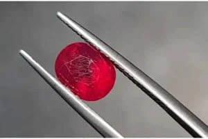
For instance, the ruby laser, one of the earliest lasers ever developed, uses a ruby crystal as its amplifying medium. When excited by external light, the atoms within the ruby crystal emit light of a specific red wavelength, producing a coherent and intense beam. Similarly, other crystals, like neodymium-doped yttrium aluminum garnet (Nd:YAG), are used to produce lasers of different wavelengths, finding applications in everything from medical surgeries to industrial cutting and engraving.
In conclusion, the intricate dance between crystal structure and optical properties is not just a subject of academic interest. It’s at the forefront of modern technological advancements, driving innovations that touch every facet of our lives. Whether it’s the vibrant display of our smartphones, the efficient lighting of our homes, or the precision tools used in industries and medicine, the silent orchestrator behind these marvels is the deep understanding of crystals and their interaction with light. As we continue to unravel the mysteries of these structures, the horizon of possibilities keeps expanding, promising a future illuminated by the confluence of science and technology.
Conclusion
The intricate relationship between a crystal’s structure and its optical properties is a testament to the wonders of materials science. By understanding this connection, we can harness the power of crystals in various technological applications, pushing the boundaries of what’s possible in the realm of optics.
FAQs
- What is the refractive index?
- It’s a measure of how much light slows down as it passes through a material.
- How does crystal structure influence color?
- The arrangement of atoms and the behavior of electrons within the crystal can determine which wavelengths of light are absorbed, leading to coloration.
- Why are some crystals transparent while others are opaque?
- This is due to differences in how light interacts with the atomic arrangement in the crystal, leading to varying degrees of absorption, reflection, and transmission.
- What role do imperfections play in a crystal’s optical properties?
- Imperfections or irregularities in the crystal lattice can cause light to scatter in various directions, influencing the crystal’s overall appearance.
- How are crystals used in laser technology?
- Specific crystal structures are used in lasers to produce light of a particular wavelength, allowing for precision in applications like medical procedures and data transmission.