LiNbO3 LN
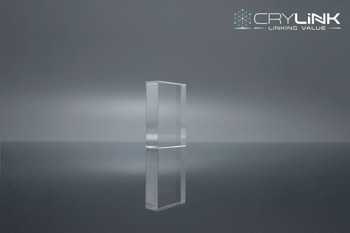
LiNbO3 Crystal For 2790 Electro-Optical Modulation
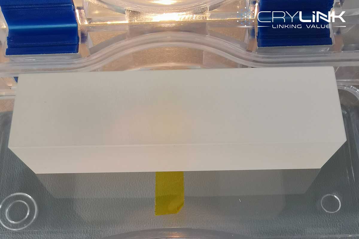
Size: 45*20*11mm
Coating: AR/AR@2790nm, R≥99%; With high threshold
- Optical Communication
532nm laser - Medical Applications
2940nm laser - Pulse range finder
- Laser target indicator
- Electro-optic Q-switch
LiNbO3 crystal has been widely used in optical waveguide and optical communication technology because of its excellent electro-optical properties. It is an ideal substrate material for many integrated optoelectronic devices. Because of the large electro-optic coefficient of LiNbO3, the half-wave voltage is low. The electro-optic effect of LiNbO3 crystal is usually used to modulate the optical signal. Electro-optic modulation is divided into longitudinal and transverse, and LiNbO3 is mainly used in transverse modulation. It has been widely used in medium and low power solid-state lasers.
- Wide transparency range
- High electro-optic efficiency
- Stable mechanical and chemical properties
- Low absorption loss
- low damage threshold
- Small volume
- Not easy to deliquesce
- High temperature stability
- Large electro-optic coefficient
- Easy to grow into large crystal
| In situ imaging ellipsometer using a LiNbO3 electrooptic crystal Thin Solid Films 571 (2014) 532–537 |
| Effects of atmosphere, metal films, temperatures and holding time on the surface topography and electrical conductivity of LiNbO3 single crystals Ceramics International |
| Design, fabrication and characterization of SAW devices on LiNbO3 bulk and ZnO thin film substrates Solid State Electronics 150 (2018) 28–34 |
| LiNbO3 integrated system for opto-microfluidic sensing Sensors & Actuators: B. Chemical 282 (2019) 391–398 |
If you can’t find the Literature you want, Contact us to get the PDF Get the Literature
| Pressure sensor based on polarization rotation in z-cut LiNbO3 optical waveguide Sensors and Actuators A 280 (2018) 521–524 |
| A comparative study for two LiNbO3 cuts (Y-Z and Y-X) in detecting bulk acoustic microwaves using Probabilistic Neural Network Engineering Science and Technology, an International Journal 21 (2018) 527–531 |
| The electromechanical features of LiNbO3 crystal for potential high temperature piezoelectric applications Journal of Materiomics 5 (2019) 73e80 |
| Growth and mechanical properties of near-stoichiometric LiNbO3 crystal Optik 164 (2018) 385–389 |
| Nonlinear-optical characterization of planar domain patterns written in LiNbO3 by electron-beam irradiation Optical Materials 75 (2018) 325e330 |
| Characterization of Mn-doped electrospun LiNbO3 nanofibers by Raman spectroscopy Materials Characterization 127 (2017) 209–213 |
| Incipient plasticity and surface damage in LiTaO3 and LiNbO3 single crystals Materials and Design 153 (2018) 221–231 |
| Controllable synthesis of LiNbO3 micro-octahedrons and micro-cubes via a molten-salt process Ceramics International 44 (2018) 22874–22879 |
| Intensity modulator fabricated in LiNbO3 by femtosecond laser writing Optics and Lasers in Engineering 111 (2018) 222–226 |
| Mode tailoring of laser written waveguides in LiNbO3 crystals by multi-scan of femtosecond laser pulses Optical Materials 86 (2018) 571–575 |
| XPS study of Li/Nb ratio in LiNbO3 crystals. Effect of polarity and mechanical processing on LiNbO3 surface chemical composition Applied Surface Science 389 (2016) 387–394 |
| Swift heavy ion irradiation induces enhancement in electrical conductivity of LiTaO3 and LiNbO3 crystals Nuclear Inst. and Methods in Physics Research B 435 (2018) 152–156 |
LiNbO3 crystals crylink have supplied
| Size (mm) | Orientation | Coating |
| Φ3×0.5 | Y-Cut | |
| Φ4×0.5 | ||
| Φ6×0.5 | 128°Y-Cut | |
| 13*11*50 | θ=48°, φ=30° | |
| 45*20*11 | AR/AR@2790nm, R≥99%; | |
| Φ90.17×1.51 |
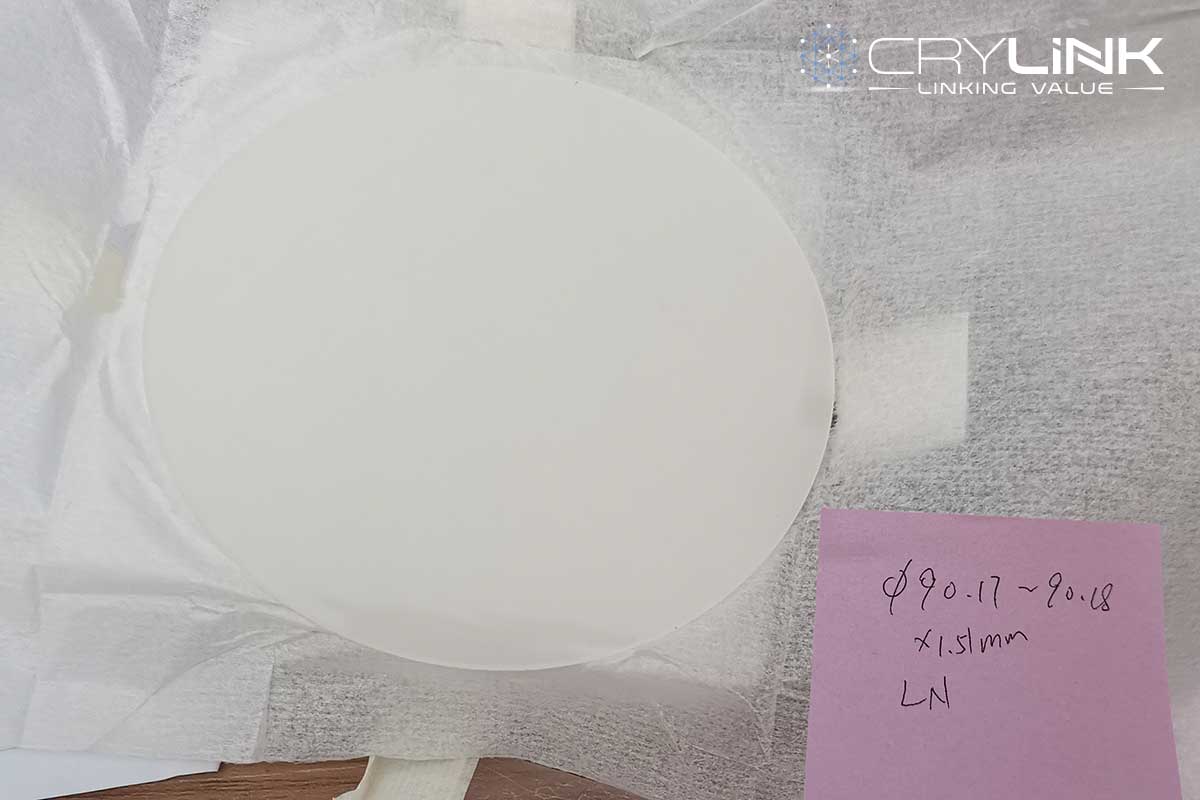
Size: ∅ (90.17-90.18)*1.51 mm
Size: ∅ (90.17-90.18)*1.51 mm
Size: ∅4*0.5mm
Both Sides Polished
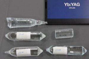
Size: 13*11*50 mm
Orientation: θ=48°, φ=30°
Both Sides Polished
Size: 13*11*50 mm
Orientation: θ=48°, φ=30°
Both Sides Polished
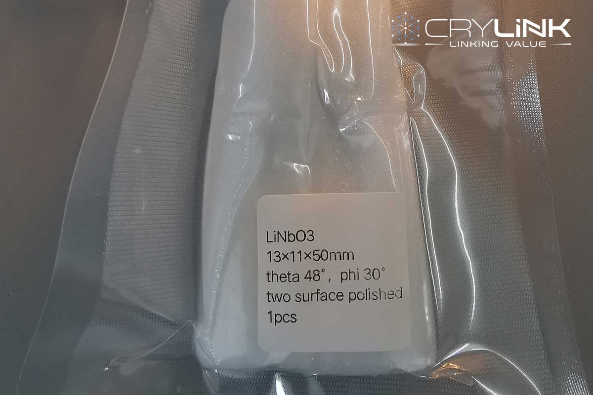
Size: 13*11*50 mm
Orientation: θ=48°, φ=30°
Both Sides Polished
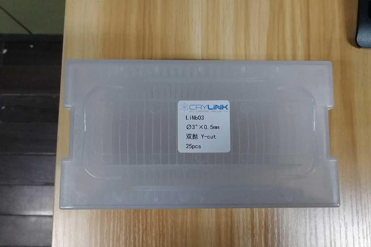
Size: ∅3*0.5mm
Orientation: Y Cut
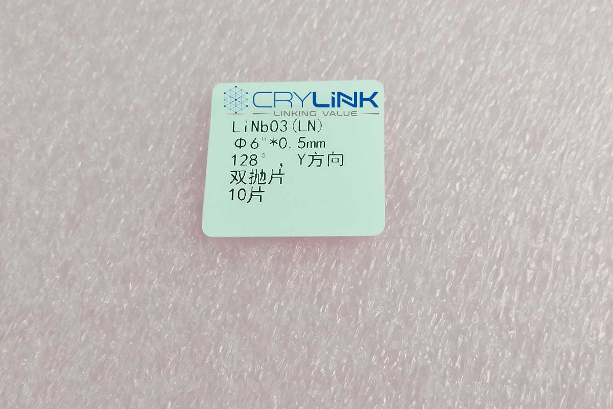
Size: ∅6*0.5mm
Orientation: 128°Y Cut
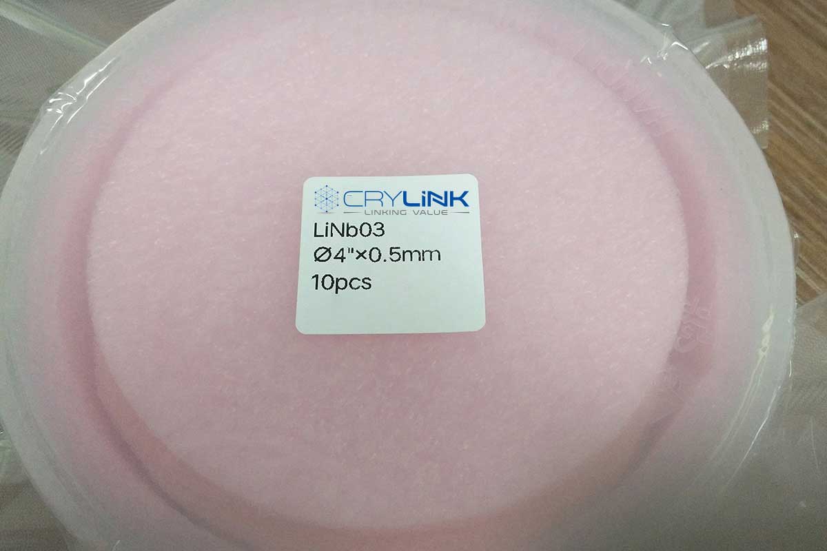
Size: ∅4*0.5mm
Both Sides Polished
Parameter
| Chemical formula | LiNbO3 |
| Crystal structure | trigonal |
| Space group | R3C |
| Density | 4.64 g/cm3 |
| Mohs hardness | 5 |
| Optical homogeneity | ~ 5 x 10⁻⁵ / cm |
| Transparency range | 420 – 5200 nm |
| Absorption coefficient | ~ 0.1 % / cm @ 1064 nm |
| Refractive indices at 1064 nm | ne = 2.146, no = 2.220 @ 1300 nm |
| ne = 2.156, no = 2.232 @ 1064 nm | |
| ne = 2.203, no = 2.286 @ 632.8 nm | |
| Sellmeier equations (λ, μm) | no2 = 4.9048 + 0.11768 / (λ2 – 0.04750) – 0.027169λ2 |
| ne2 = 4.5820 + 0.099169 / (λ2 – 0.04443) – 0.021950λ2 | |
| Thermal expansion coefficient @ 25 °C | //a, 2.0 x 10⁻⁶ / K |
| //c, 2.2 x 10⁻⁶ / K | |
| Thermal conductivity | ~ 5 W/m/K @ 25 °C |
| Thermal optical coefficient | dno/dT = -0.874 x 10⁻⁶ / K at 1.4 µm |
| dne/dT = 39.073 x 10⁻⁶ / K at 1.4 µm |
| Refractive retardation | Γ=лLnr22V/λd |
| Electro-optic coefficients | R33=32pm/V |
| R31=10pm/V | |
| R22=6.8 pm/V | |
| Aperture | 4x4mm ~ 9x9mm |
| Length | 15~25mm |
| Tolerance of size | +/-0.1mm |
| Chamfer | <0.5mm x 45° |
| Accuracy of orientation | <5 arc min |
| Parallelism | <10 arc sec |
| Flatness | l/8 at 632.8 nm |
| Wavefront Distortion | <l/4 at 632.8 nm |
| Extinction Ratio | >400:1 @ 633nm, dia 6mm beam |
| Operating wavelength range | 1.525-1.605μm |
| Extinction ratio | <20dB |
| Half wave voltage | <6V |
| DC bias voltage | <8V |
| Input characteristic impedance | 50Ω |
| Light reflection | ≤-50dB |
| Maximum input electric power | 20dBm |
| Maximum input optical power | 10-100mW |
| Storage temperature | -40-85℃ |
| Operating temperature | -40-70℃ |
| Elastic Stiffness Coefficient cij/(1010N/m2) | c11 | c12 | c13 | c14 | c33 | c44 |
| 20.3 | 5.3 | 7.5 | 0.9 | 24.5 | 6.0 | |
| Elastic Compliance Coefficient sij/(10-12m2/N) | S11 | S12 | S13 | S14 | S33 | S44 |
| 5.78 | -1.01 | -1.47 | -1.02 | 5.02 | 17.0 |
| Piezoelectric Strain Constantdij/(10-11C/N) | d11 | d15 | d22 | d31 | d33 |
| 8 | 7.4 | 2.04 | -0.086 | 1.62 |
| Dielectric Constant | εT11/ε0 | εT11/ε0 |
| 78 | 32 | |
| Electromechanical Coupling Coefficient kij(%) | k15 | k31 |
| 68 | 50 |
| NLO Coefficients | d33 = 34.4 pm/V |
| d31 = d15 = 5.95 pm/V | |
| d22 = 3.07 pm/V | |
| Efficiency NLO Coefficients | deff =5.7 pm/V or ~14.6 x d36 (KDP) for frequency doubling 1300 nm; |
| deff =5.3 pm/V or ~13.6 x d36 (KDP) for OPO pumped at 1064 nm; | |
| deff =17.6 pm/V or ~45 x d36 (KDP) for quasi-phase-matched structure. | |
| Electro-Optic Coefficients | gT33 = 32 pm/V, gS33 = 31 pm/V, |
| gT31 =10 pm/V, gS31=8.6 pm/V, | |
| gT22 = 6.8 pm/V, gS22= 3.4 pm/V, | |
| Half-Wave Voltage, DC Electrical field||z, light ^z: Electrical field||x or y, light||z: | 3.03 KV |
| 4.02 KV | |
| Damage Threshold | 100 MW/cm2 (10 ns, 1064nm) |
| Transmitted wavefront distortion | better than l/4 @ 633nm |
| Dimension tolerance | (W±0.1mm) x (H±0.1mm) x (L±0.2mm) |
| Clear aperture | over 90% central diameter |
| Flatness | l/8 @ 633nm |
| Surface quality | 20 /10 Scratch/Dig |
| Parallelism | better than 20 arc sec |
| Perpendicularity | 5 arc min |
| Angle tolerance | Dq < 0.5o, Df < 0.5o |
| AR-coating | dual wave band AR coating at 1064/532 nm on both surfaces, with R < 0.2% at 1064 nm and R < 0.5% at 0.532 nm per surface |