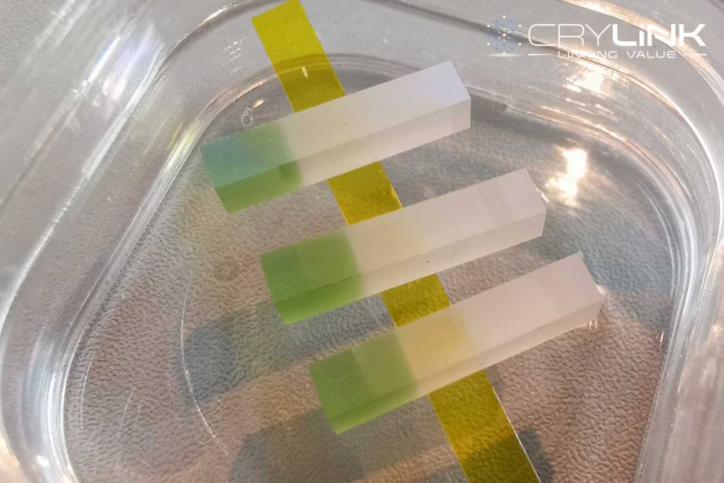
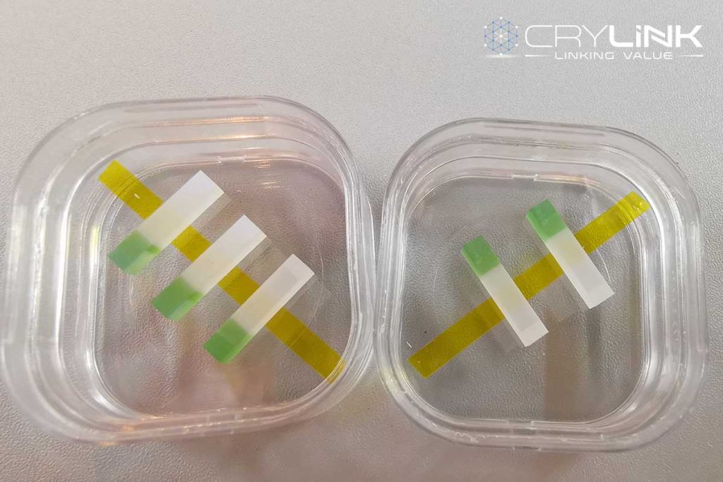
Search
Close this search box.

Nd:YAG+V:YAG Bonding Crystal

Specifications
ProductSize/mmQuantity /pcs
Nd:YAG+V:YAG Microchip2.8*2.8*14.3mm6
Processing Requirements
  • Nd:YAG + V:YAG microchip
  • Size: 2.8*2.8*14.2mm
  • Nd:YAG:10mm;
  • V:YAG:4.2mm, T0=75%@1319nm
Coating Requirements
  • Nd:YAG Surface:
    R <1% @808±5nm & R > 99.9% @1319±1nm & R<10% @1064±1nm ,AOI=0±5°;
  • V:YAG Surface:
    R=85%±2% @1319±1nm & R<10% @1064±1nm, AOI=0±5°
    Damage Threshold>700MW/cm2@10ns,10Hz,1319nm
Coating Test Curve
1064NM
Reflection Spectrum of Nd:YAG Crystal
1319NM
Reflection Spectrum of V:YAG Crystal
Product Images
Nd-YAG+V-YAG
Nd-YAG-V-YAG
Jackie Dong

Jackie Dong

In photonic crystals, nanophotonics, negative refraction media, surface plasma optics, nonlinear optics and quantum optics, he has made many innovative achievements in theoretical and experimental research on electromaanetic field problems.

Table of Contents

Related Post

would be happy to meet you and learn all about your requirements & expectations.

celia
Celia Cheng
never
Never Xiong

Contact Us Today, Get Reply Tomorrow

Your information will be kept strictly confidential.

I am Ben Fang, the CEO of laser-crylink.com, me and my team would be happy to meet you and learn all about your business, requirements and expectations.