Introduction
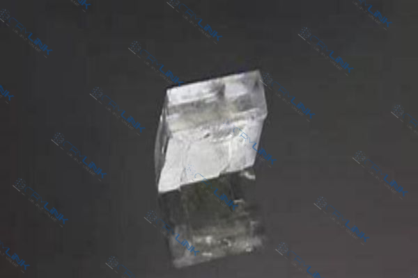
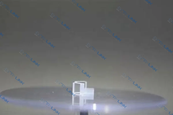
Crystals are solid materials in which the atoms, ions, or molecules are arranged in an orderly repeating pattern extending in all three spatial dimensions. The study of crystals and their structure is a cornerstone in the fields of mineralogy and materials science. In this article, we delve deep into the fascinating world of crystals, exploring their formation process and the various types of crystal structures.
The Crystallization Process
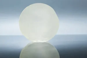
Crystallization is a fascinating and intricate process that plays a pivotal role in various scientific and industrial applications. At its core, crystallization is the transformation of a substance from a disordered or fluid state into a highly ordered, solid crystalline structure. This transformation is not only visually captivating, as seen in the formation of snowflakes or gemstones, but also fundamental to many manufacturing and purification processes.
When we delve into the concept of crystallization, we find that it’s not just a simple transition from liquid to solid. Instead, it’s a complex interplay of molecular interactions, thermodynamics, and kinetics. The resulting crystal is a testament to nature’s ability to organize atoms or molecules in a highly symmetrical and repeating pattern, extending in all three spatial dimensions.
One of the primary drivers of crystallization is the change in temperature. As a solution cools, the solubility of the solute often decreases. This means that, at lower temperatures, the solution can no longer hold as much of the solute in its dissolved state as it could at higher temperatures. As a result, the excess solute molecules start to come together, forming a solid crystal. This is commonly observed when making rock candy, where sugar crystals form as a supersaturated sugar solution cools.
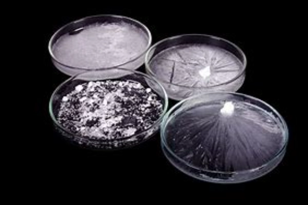
Speaking of supersaturation, it’s another crucial factor in the crystallization process. A solution becomes supersaturated when it contains more dissolved solute than it would under equilibrium conditions at that temperature. In such a state, the solution is teetering on the edge, looking for the slightest nudge to start the crystallization process. This nudge can come in the form of a seed crystal, a speck of dust, or even a disturbance like stirring. Once initiated, the crystallization in a supersaturated solution can be rapid and dramatic.
However, not all crystallization is desired or beneficial. The presence of impurities can significantly impact the process. These foreign substances can either inhibit crystallization, making it harder for the desired crystal to form, or they can act as seed points, promoting the formation of many small, often undesired, crystals. This is why, in industries where crystal size and purity are crucial, such as in the pharmaceutical sector, controlling impurities is of paramount importance.
In conclusion, the crystallization process is a delicate balance of various factors. Whether it’s the mesmerizing formation of snowflakes in winter, the growth of beautiful gemstones deep within the Earth, or the purification of substances in a laboratory, understanding and harnessing the principles of crystallization is essential. Through a deeper appreciation of this process, we can better utilize it in various applications, from making better medicines to creating more efficient electronic materials.
Types of Crystal Structures
The world of crystal structures is as diverse as it is fascinating. These structures, which are the arrangement of atoms or molecules in a crystalline material, play a crucial role in determining the properties of materials. From the hardness of a diamond to the conductivity of metals, the underlying crystal structure is a key determinant.
Starting with the Simple Cubic Structure (SCS), this is the most basic form of crystal arrangement. Imagine a cube, and at every corner of this cube, there’s an atom. While this structure is easy to visualize and understand, it’s not the most efficient way to pack atoms together. There’s a lot of empty space in between, which means materials with this structure may not have the densest or strongest properties.
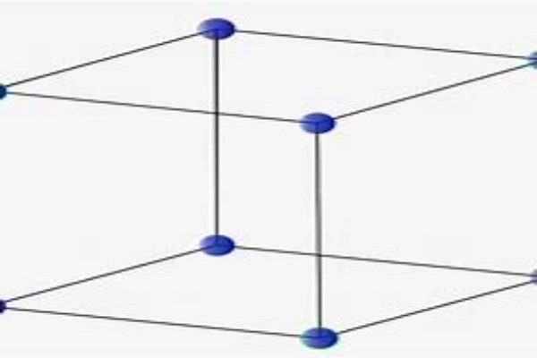
On the other hand, the Body-Centered Cubic Structure (BCC) offers a more compact arrangement. In addition to the atoms at the corners of the cube, there’s one right in the center. This central atom significantly reduces the empty space, leading to materials that are denser and often stronger than those with a simple cubic structure. Many metals, like iron at room temperature, adopt this structure.
The Face-Centered Cubic Structure (FCC) takes atom packing to another level. In this arrangement, atoms are not only at the corners of the cube but also at the center of each face. This results in a very tight packing of atoms, minimizing the empty spaces. It’s no wonder that many metals, including gold, silver, and aluminum, have this structure. These metals are known for their malleability, and the FCC structure plays a role in that.
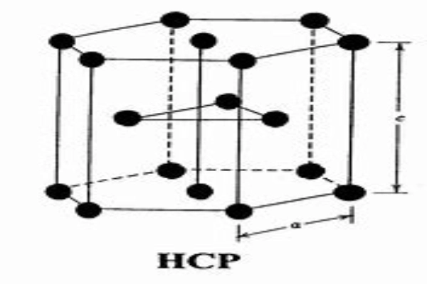
The Hexagonal Close-Packed Structure (HCP) is a bit different from the cubic structures. As the name suggests, it’s based on a hexagonal geometry. The atoms are arranged in a way that they form a repeating pattern of hexagons, with an additional atom in the center. This structure is prevalent in metals like zinc and magnesium. The unique arrangement gives these metals specific properties, like the ability to withstand certain types of stress.
Lastly, the Diamond Cubic Structure is truly special. It’s the structure that gives diamonds, the hardest natural material known, its remarkable properties. In this arrangement, each carbon atom is connected to four others, forming a tetrahedron. This three-dimensional network of strong carbon-carbon bonds ensures that diamonds are incredibly hard and almost impossible to scratch.
In essence, the arrangement of atoms in a material, its crystal structure, is a significant factor in determining its properties. Whether it’s the luster of gold, the strength of iron, or the brilliance of a diamond, the underlying crystal structure plays a pivotal role. By understanding these structures, scientists and engineers can tailor materials for specific applications, leading to innovations in everything from electronics to aerospace.
Applications of Crystals in Modern Technology
Crystals, with their ordered and repetitive atomic structures, have become indispensable in today’s technologically driven world. Their unique properties, ranging from electrical conductivity to optical characteristics, have paved the way for innovations that touch almost every aspect of our daily lives.
In the realm of electronics, silicon crystals stand out as the backbone of the semiconductor industry. These crystals provide the foundation for integrated circuits found in everything from smartphones to computers. The purity and structural perfection of silicon crystals allow for the miniaturization of electronic components, leading to devices that are both powerful and compact. As technology continues to evolve, the demand for even more refined and high-quality silicon crystals grows, driving advancements in crystal growth techniques.
Beyond silicon, other crystals like gallium arsenide and gallium nitride are making their mark in specialized electronic applications. These materials offer advantages in terms of speed and efficiency, especially in high-frequency applications like satellite communication and radar systems.
In the medical field, crystals play a pivotal role in diagnostic imaging. Certain crystals, when struck by X-rays or gamma rays, emit light in a process known as scintillation. This property is harnessed in devices like PET scanners, where crystals convert radiation into visible light, creating detailed images of the body’s interior. This non-invasive imaging technique has revolutionized the diagnosis and treatment of various diseases, providing insights that were previously unattainable.
Furthermore, piezoelectric crystals, which generate voltage when subjected to mechanical stress, have found applications in ultrasound imaging. When these crystals are electrically stimulated, they produce sound waves that, upon reflection, create detailed images of soft tissues, aiding in prenatal care and cardiac assessments.
In the realm of data storage and communication, optical crystals are used in fiber optics technology. These crystals guide light signals over long distances with minimal loss, enabling high-speed internet and telecommunications.
In conclusion, the applications of crystals in modern technology are vast and varied. As we continue to uncover the potential of different crystalline materials, it’s evident that their role in shaping the future of technology is both significant and enduring.
Conclusion
Crystals, with their diverse structures and unique properties, play a pivotal role in both nature and technology. Understanding the intricacies of their formation and the different types of crystal structures is crucial for advancements in various scientific and industrial fields.
FAQs
- What is the primary difference between BCC and FCC structures?
- The main difference lies in the arrangement of atoms. In BCC, there’s an atom at the cube’s center, while in FCC, there are atoms in the center of each face of the cube.
- How does temperature influence crystallization?
- A decrease in temperature can lead to the formation of crystals as it may reduce the solubility of a substance.
- Why are silicon crystals essential in the semiconductor industry?
- Silicon crystals have properties that make them ideal for use in electronic devices, especially in the creation of semiconductors.
- What makes the diamond cubic structure so durable?
- The tetrahedral arrangement of carbon atoms in the diamond cubic structure results in a very hard and durable crystal.
- Are all crystals visible to the naked eye?
- No, many crystals are microscopic and require specialized equipment to be observed.